
TSMC's new packaging technology will bring down chip cost and improve performance
- Posted on June 12, 2026, 2 p.m.
TSMC's Revolutionary CoPoS Packaging Set to Transform Chip Performance and Cost by 2028
TSMC, the world's leading contract chip manufacturer, is on the cusp of a significant breakthrough in semiconductor technology with its innovative CoPoS packaging. Sources close to the development indicate that CoPoS, an acronym for Chip-on-Panel-on-Structure, is poised to redefine chip manufacturing as we know it.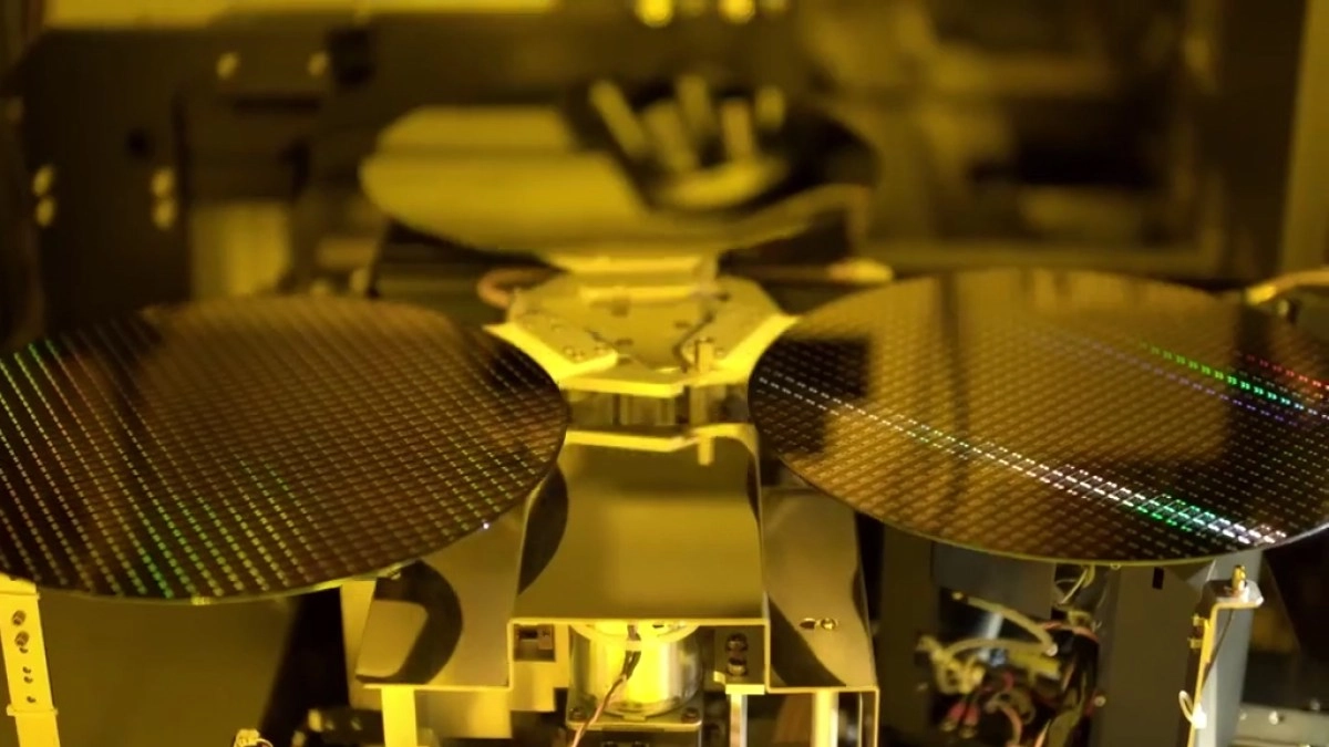
What is CoPoS?
At its core, CoPoS leverages a unique glass material that serves a dual purpose: acting as a temporary carrier during the manufacturing process and integrating into the final chip substrate. This creates a sophisticated three-layer "sandwich" structure, enabling unprecedented levels of integration and efficiency.
The Impact of CoPoS: Cost Reduction and Performance Gains
The implications of CoPoS are far-reaching. TSMC anticipates that by the end of 2028, when mass production is slated to begin, this new packaging technology will lead to a substantial reduction in manufacturing costs. Simultaneously, CoPoS is engineered to deliver significant improvements in chip performance, a crucial factor in the ever-evolving landscape of high-demand computing.
AI and High-Performance Computing: The First to Benefit
The primary beneficiaries of TSMC's CoPoS technology will be those at the forefront of technological advancement. Specifically, Nvidia's upcoming Feynman AI chipset is set to be the inaugural recipient of this cutting-edge packaging. This strategic rollout highlights TSMC's focus on empowering the next generation of AI and high-performance computing (HPC) chips with the enhanced capabilities that CoPoS provides.
Source
0 Responses Write a Response